- Home
- Services/IndustriesServicesindustries
- About Us
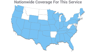
- LocationsStatesAccordion ContentAccordion ContentAccordion ContentAccordion Content
- Job Openings
- Quick Links
- ATS Family
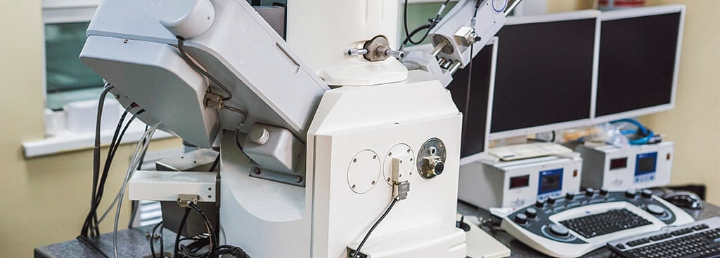
SEM Lab
Applied Technical Services’ SEM lab provides high-resolution imaging ideal for failure analysis and other metallurgy services.
What is SEM, and Why is it Important?
Scanning Electron Microscopy is a common material’s science technique where the image of a material’s surface is magnified for further analysis. SEM allows magnifications to reach up to 300,000X, providing information about the sample material’s topography, morphology, and composition. The high-resolution imaging is ideal for various applications, including:
- Chemical Characterization of Surfaces
- Digital Image Analysis
- Failure Analysis
- Fractography
- Litigation Support
- Microstructure Analysis
- Quantitative and Qualitative (when paired with an EDS)
- Particle Analysis
SEM is an effective investigative tool that highlights the microscopic details of materials. Scanning electron microscopy is useful in research and development as it allows manufacturers to further their understanding of a material’s composition, potential uses, and failures. ATS provides SEM lab services for the following industries.
- Aerospace
- Automotive
- Chemistry
- Construction
- Energy
- Manufacturing
Applied Technical Services' SEM Analysis Lab
- Contaminants
- Coatings
- Corrosion Products
- Elemental Mapping
- General Alloy ID
- Polymer Filler Material ID
- Platings
- Wear Metals
The Advantages of Scanning Electron Microscopy
SEM has several advantages, including:
- Quick results
- Comprehensive chemical analysis
- High-resolution imaging
- Improved depth of field
- Universal standards of measurements
- Applicable to several materials; including metals, polymers, ceramics, and alloys
About Applied Technical Services
ATS has offered high-quality engineering consulting, inspection, and testing services since 1967. As an ISO 9001 certified management system, we provide proven and professional services to clients in dozens of disciplines across the globe. Our staff consists of metallurgists, chemists, engineers, and other professionals with decades of combined professional experience. Our labs uphold the latest industry standards and practices and provide clients with clear, concise, and accurate reports. Call +1 (888) 287-5227 and request a free quote from our SEM lab.
Request Form
"*" indicates required fields
Complete List Of Metallurgy Links
- 3D Inspections
- 3D Part Inspection
- 3D Scanning Services
- 3D X-Ray Imaging
- 3D X-Ray Services
- Computed Tomography
- Computed Tomography Lab
- Computed Tomography Metallurgy
- Computed Tomography Scanning
- Computed Tomography (CT) Services
- CT 3D Scanning for Reverse Engineering
- CT Inspections
- CT Lab
- CT Metrology
- CT Scan Companies
- CT Scan Parts
- CT Services
- First Article CT Scanning
- X-Ray Microtomography
General Services
- EDS Chemical Analysis
- Litigation Support
- Material Identification
- Metallography Lab
- SEM Lab
- Metallurgical Services
- Nondestructive Hardness Testing
- Porosity Analysis
- PPE Testing
- Reverse Engineering Services
- Scanning Electron Microscopy
- Scanning Electron Microscope Services
- Tensile Testing Metallurgical Lab
Metals Testing and Metallography
- Brinell Hardness Tests
- Case Depth Hardness
- Case Depth Testing
- Fracture Analysis
- Fracture Surface Analysis
- Grain Size Analysis
- Grain Size Distribution
- Hardness Testing Labs
- Hardness Testing Services
- Intergranular Corrosion Tests
- Knoop Hardness Testing
- Laser Grain Size Analysis
- Metal Tests
- Metal Fracture Analysis
- Metallurgical Testing Services
- Metallography Lab
- Metallography Microstructure and Analysis
- Rockwell Hardness Tests
- Superficial Rockwell Hardness Tests
- Vickers Hardness Test